Friday, November 20, 2015

Insulator


Insulator:
An electrical insulator is a material whose internal electric charges do not flow freely, and therefore make it nearly impossible to conduct an electric current under the influence of an electric field. This contrasts with other materials, semiconductors and conductors, which conduct electric current more easily. The property that distinguishes an insulator is its resistivity; insulators have higher resistivity than semiconductors or conductors.

A perfect insulator does not exist, because even insulators contain small numbers of mobile charges (charge carriers) which can carry current. In addition, all insulators become electrically conductive when a sufficiently large voltage is applied that the electric field tears electrons away from the atoms. This is known as the breakdown voltage of an insulator. Some materials such as glass, paper and Teflon, which have high resistivity, are very good electrical insulators. A much larger class of materials, even though they may have lower bulk resistivity, are still good enough to prevent significant current from flowing at normally used voltages, and thus are employed as insulation for electrical wiring and cables. Examples include rubber-like polymers and most plastics.

Insulators are used in electrical equipment to support and separate electrical conductors without allowing current through themselves. An insulating material used in bulk to wrap electrical cables or other equipment is called insulation. The term insulator is also used more specifically to refer to insulating supports used to attach electric power distribution or transmission lines to utility poles and transmission towers. They support the weight of the suspended wires without allowing the current to flow through the tower to ground.


Types of insulators:
1. Pin Insulator
2. Suspension Insulator
3. Strain Insulator
4. Shackle Insulator


Pin Insulator:

Pin Insulator is earliest developed overhead insulator, but still popularly used in power network up to 33KV system. Pin type insulator can be one part, two parts or three parts type, depending upon application voltage. In 11KV system we generally use one part type insulator where whole pin insulator is one piece of properly shaped porcelain or glass. As the leakage path of insulator is through its surface, it is desirable to increase the vertical length of the insulator surface area for lengthening leakage path. In order to obtain lengthy leakage path, one, tow or more rain sheds or petticoats are provided on the insulator body. In addition to that rain shed or petticoats on an insulator serve another purpose. These rain sheds or petticoats are so designed, that during raining the outer surface of the rain shed becomes wet but the inner surface remains dry and non-conductive. So there will be discontinuations of conducting path through the wet pin insulator surface.
In higher voltage like 33KV and 66KV manufacturing of one part porcelain pin insulator becomes difficult. Because in higher voltage, the thickness of the insulator become more and a quite thick single piece porcelain insulator can not manufactured practically. In this case we use multiple part pin insulator, where a number of properly designed porcelain shells are fixed together by Portland cement to form one complete insulator unit. For 33KV tow parts and for 66KV three parts pin insulator are generally used.


Suspension Insulator:
In higher voltage, beyond 33KV, it becomes uneconomical to use pin insulator because size, weight of the insulator become more. Handling and replacing bigger size single unit insulator are quite difficult task. For overcoming these difficulties, suspension insulator was developed.
In suspension insulator numbers of insulators are connected in series to form a string and the line conductor is carried by the bottom most insulator. Each insulator of a suspension string is called disc insulator because of their disc like shape.  


Strain Insulator:
When suspension string is used to sustain extraordinary tensile load of conductor it is referred as string insulator. When there is a dead end or there is a sharp corner in transmission line, the line has to sustain a great tensile load of conductor or strain. A strain insulator must have considerable mechanical strength as well as the necessary electrical insulating properties.  


Shackle Insulator:

The shackle insulator or spool insulator is usually used in low voltage distribution network. It can be used both in horizontal and vertical position. The use of such insulator has decreased recently after increasing the using of underground cable for distribution purpose. The tapered hole of the spool insulator distributes the load more evenly and minimizes the possibility of breakage when heavily loaded. The conductor in the groove of shackle insulator is fixed with the help of soft binding wire.

arduino uno datasheet with atmega328p


Thursday, November 19, 2015

resistance


The electrical resistance of an electrical conductor is a measure of the difficulty to pass an electric current through that conductor. The inverse quantity is electrical conductance, the ease with which an electric current passes. Electrical resistance shares some conceptual parallels with the notion of mechanical friction. The SI unit of electrical resistance is the ohm (Ω), while electrical conductance is measured in siemens (S).
An object of uniform cross section has a resistance proportional to its resistivity and length and inversely proportional to its cross-sectional area. All materials show some resistance, except for superconductors, which have a resistance of zero.
The resistance (R) of an object is defined as the ratio of voltage across it (V) to current through it (I), while the conductance (G) is the inverse:
R = {V\over I}, \qquad G = {I\over V} = \frac{1}{R}
For a wide variety of materials and conditions, V and I are directly proportional to each other, and therefore R and G are constant(although they can depend on other factors like temperature or strain). This proportionality is called Ohm's law, and materials that satisfy it are called "Ohmic" materials.
In other cases, such as a diode or battery, V and I are not directly proportional. The ratio V/I is sometimes still useful, and is referred to as a "chordal resistance" or "static resistance", since it corresponds to the inverse slope of a chord between the origin and an I–V curve. In other situations, the derivative  \frac{dV}{dI} \,\! may be most useful; this is called the "differential resistance".

Friday, November 13, 2015

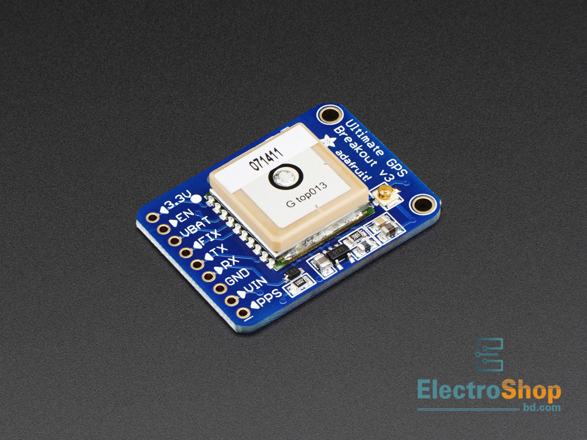
MTK3339 Ultimate GPS Breakout - 66 ch. W/10 Hz module -V.3

-165 dBm sensitivity, 10 Hz updates, 66 channels
5V friendly design and only 20mA current draw
Breadboard friendly + two mounting holes
RTC battery-compatible
Built-in datalogging
PPS output on fix
We have received reports that it works up to ~32Km altitude (the GPS theoretically does not have a limit until 40Km)
Internal patch antenna + u.FL connector for external active antenna
Fix status LED


The breakout is built around the MTK3339 chipset, a no-nonsense, high-quality GPS module that can track up to 22 satellites on 66 channels, has an excellent high-sensitivity receiver (-165 dB tracking!), and a built in antenna. It can do up to 10 location updates a second for high speed, high sensitivity logging or tracking. Power usage is incredibly low, only 20 mA during navigation.

Best of all, we added all the extra goodies you could ever want: a ultra-low dropout 3.3V regulator so you can power it with 3.3-5VDC in, 5V level safe inputs, ENABLE pin so you can turn off the module using any microcontroller pin or switch, a footprint for optional CR1220 coin cell to keep the RTC running and allow warm starts and a tiny bright red LED. The LED blinks at about 1Hz while it's searching for satellites and blinks once every 15 seconds when a fix is found to conserve power. If you want to have an LED on all the time, we also provide the FIX signal out on a pin so you can put an external LED on.

Two features that really stand out about version 3 MTK3339-based module is the external antenna functionality and the the built in data-logging capability. The module has a standard ceramic patch antenna that gives it -165 dB sensitivity, but when you want to have a bigger antenna, you can snap on any 3V active GPS antenna via the uFL connector. The module will automatically detect the active antenna and switch over! Most GPS antennas use SMA connectors so you may want to pick up one of our uFL to SMA adapters.

The other cool feature of the MTK3339-based module (which we have tested with great success) is the built in datalogging ability. Since there is a microcontroller inside the module, with some empty FLASH memory, the newest firmware now allows sending commands to do internal logging to that FLASH. The only thing is that you do need to have a microcontroller send the "Start Logging" command. However, after that message is sent, the microcontroller can go to sleep and does not need to wake up to talk to the GPS anymore to reduce power consumption. The time, date, longitude, latitude, and height is logged every 15 seconds and only when there is a fix. The internal FLASH can store about 16 hours of data, it will automatically append data so you don't have to worry about accidentally losing data if power is lost. It is not possible to change what is logged and how often, as its hardcoded into the module but we found that this arrangement covers many of the most common GPS datalogging requirements.

Monday, November 9, 2015

Silicon is a chemical element with symbol Si and atomic number 14. It is a tetravalent metalloid, more reactive than germanium, the metalloid directly below it in the table. Controversy about silicon's character dates to its discovery; it was first prepared and characterized in pure form in 1823. In 1808, it was given the name silicium (from Latin: silex, hard stone or flint), with an -iumword-ending to suggest a metal, a name which the element retains in several non-English languages. However, its final English name, first suggested in 1817, reflects the more physically similar elements carbon and boron.
Silicon is the eighth most common element in the universe by mass, but very rarely occurs as the pure free element in nature. It is most widely distributed in dusts, sands, planetoids, and planets as various forms of silicon dioxide (silica) or silicates. Over 90% of the Earth's crust is composed of silicate minerals, making silicon the second most abundant element in the Earth's crust (about 28% by mass) after oxygen.[9]
Most silicon is used commercially without being separated, and indeed often with little processing of compounds from nature. These include direct industrial building-use of clays, silica sand and stone. Silicate goes into Portland cement for mortar andstucco, and when combined with silica sand and gravel, to make concrete. Silicates are also in whiteware ceramics such asporcelain, and in traditional quartz-based soda-lime glass and many other specialty glasses. More modern silicon compounds such as silicon carbide form abrasives and high-strength ceramics. Silicon is the basis of the widely used synthetic polymers called silicones.
Elemental silicon also has a large impact on the modern world economy. Although most free silicon is used in the steel refining,aluminium-casting, and fine chemical industries (often to make fumed silica), the relatively small portion of very highly purified silicon that is used in semiconductor electronics (< 10%) is perhaps even more critical. Because of wide use of silicon inintegrated circuits, the basis of most computers, a great deal of modern technology depends on it.
Silicon is an essential element in biology, although only tiny traces of it appear to be required by animals.[10] However, varioussea sponges as well as microorganisms like diatoms and radiolaria secrete skeletal structures made of silica. Silica is often deposited in plant tissues, such as in the bark and wood of Chrysobalanaceae and the silica cells and silicified trichomes ofCannabis sativa, horsetails and many grasses

Thursday, October 8, 2015

Breadboard

A breadboard is a construction base for prototyping of electronics. Originally it was literally a bread board, a polished piece of wood used for slicing bread. In the 1970s the solderless breadboard (AKA plugboard, a terminal array board) became available and nowadays the term "breadboard" is commonly used to refer to these. "Breadboard" is also a synonym for "prototype".

Because the solderless breadboard does not require soldering, it is reusable. This makes it easy to use for creating temporary prototypes and experimenting with circuit design. For this reason, solderless breadboards are also extremely popular with students and in technological education. Older breadboard types did not have this property. A stripboard (veroboard) and similar prototyping printed circuit boards, which are used to build semi-permanent soldered prototypes or one-offs, cannot easily be reused. A variety of electronic systems may be prototyped by using breadboards, from small analog and digital circuits to complete central processing units (CPUs).


Evolution:

This 1920s TRF radio manufactured by Signal was constructed on a wooden breadboard.
In the early days of radio, amateurs nailed bare copper wires or terminal strips to a wooden board (often literally a board to slice bread on) and soldered electronic components to them.[1] Sometimes a paper schematic diagram was first glued to the board as a guide to placing terminals, then components and wires were installed over their symbols on the schematic. Using thumbtacks or small nails as mounting posts was also common.

Breadboards have evolved over time, with the term now being used for all kinds of prototype electronic devices. For example, US Patent 3,145,483,[2] filed in 1961 and granted in 1964, describes a wooden plate breadboard with mounted springs and other facilities. US Patent 3,496,419,[3] filed in 1967 and granted in 1970, refers to a particular printed circuit board layout as a Printed Circuit Breadboard. Both examples refer to and describe other types of breadboards as prior art.

The breadboards
most commonly used today is usually made of white plastic and is a pluggable (solderless) breadboard. It was designed by Ronald J. Portugal of EI Instruments Inc. in 1971.[4]

Alternatives:

Wire wrap backplane
Alternative methods to create prototypes are point-to-point construction (reminiscent of the original wooden breadboards), wire wrap, wiring pencil, and boards like the stripboard. Complicated systems, such as modern computers comprising millions of transistors, diodes, and resistors, do not lend themselves to prototyping using breadboards, as their complex designs can be difficult to lay out and debug on a breadboard.

Modern circuit designs are generally developed using a schematic capture and simulation system, and tested in software simulation before the first prototype circuits are built on a printed circuit board. Integrated circuit designs are a more extreme version of the same process: since producing prototype silicon is costly, extensive software simulations are performed before fabricating the first prototypes. However, prototyping techniques are still used for some applications such as RF circuits, or where software models of components are inexact or incomplete.

You could also use a square grid of pairs of holes where one hole per pair connects to its row and the other connects to its column. This same shape can be in a circle with rows and columns each spiraling opposite clockwise/counterclockw

Bus and terminal strips:

The hole pattern for a typical etched prototyping PCB (printed circuit board) is similar to the node pattern of the solderless breadboards shown above.
Solderless breadboards are available from several different manufacturers, but most share a similar layout. The layout of a typical solderless breadboard is made up from two types of areas, called strips. Strips consist of interconnected electrical terminals.

Terminal strips:
The main areas, to hold most of the electronic components.
In the middle of a terminal strip of a breadboard, one typically finds a notch running in parallel to the long side. The notch is to mark the centerline of the terminal strip and provides limited airflow (cooling) to DIP ICs straddling the centerline[citation needed]. The clips on the right and left of the notch are each connected in a radial way; typically five clips (i.e., beneath five holes) in a row on each side of the notch are electrically connected. The five clip columns on the left of the notch are often marked as A, B, C, D, and E, while the ones on the right are marked F, G, H, I and J. When a "skinny" dual in-line pin package (DIP) integrated circuit (such as a typical DIP-14 or DIP-16, which have a 0.3-inch (7.6 mm) separation between the pin rows) is plugged into a breadboard, the pins of one side of the chip are supposed to go into column E while the pins of the other side go into column F on the other side of the notch.
Bus strips:
To provide power to the electronic components.
A bus strip usually contains two columns: one for ground and one for a supply voltage. However, some breadboards only provide a single-column power distributions bus strip on each long side. Typically the column intended for a supply voltage is marked in red, while the column for ground is marked in blue or black. Some manufacturers connect all terminals in a column. Others just connect groups of, for example, 25 consecutive terminals in a column. The latter design provides a circuit designer with some more control over crosstalk (inductively coupled noise) on the power supply bus. Often the groups in a bus strip are indicated by gaps in the color marking.
Bus strips typically run down one or both sides of a terminal strip or between terminal strips. On large breadboards additional bus strips can often be found on the top and bottom of terminal strips.
Some manufacturers provide separate bus and terminal strips. Others just provide breadboard blocks which contain both in one block. Often breadboard strips or blocks of one brand can be clipped together to make a larger breadboard.

In a more robust variant, one or more breadboard strips are mounted on a sheet of metal. Typically, that backing sheet also holds a number of binding posts. These posts provide a clean way to connect an external power supply. This type of breadboard may be slightly easier to handle. Several images in this article show such solderless breadboards.

Saturday, October 3, 2015

push switch

Low-current, momentary action pushbutton switches, such as PCB-mount 'tactile' types, are cheap, and available in an abundance of different styles. Latching types, on the other hand, are often larger, more expensive, and available only in a relatively limited range of styles. This can be a problem if you need a small, inexpensive switch for latching power to a load. The solution is to convert a pushbutton's momentary action into a latching function.
Previous Design Ideas have proposed solutions based on discrete components (Ref. 1) and IC-based circuits (Ref.2 and Ref.3). The circuit outlined below, however, requires just two transistors and a handful of passive components to achieve the same result.
The circuit in Figure 1(a) is configured to latch power to a low-side (ground-referred) load. It works in 'toggle' mode; that is, the first switch closure applies power to the load, the second removes power, and so on.
SPONSOR VIDEO, MOUSEOVER FOR SOUND
Figure 1  Circuit converts momentary action push switch into latching power switch.
To understand how the circuit operates, assume that the DC power supply, +VS, has just been applied, capacitor C1 is initially uncharged, and Q1 is off. The P-channel MOSFET, Q2, is held in its off state by R1 and R3, which work in series to pull the gate up to +VS, such that VGS is zero. The circuit is now in its 'unlatched' state, where the load voltage, VL, at the OUT (+) terminal is zero.
If the normally-open push switch is momentarily closed, C1 – being uncharged – pulls Q2's gate to 0V, thus turning on the MOSFET. The load voltage at OUT (+) now rises immediately toward +VS , and Q1 receives base bias via R4 and turns on. Under these conditions, Q1 saturates and pulls Q2's gate low via R3, thus holding the MOSFET on when the switch has opened. The circuit is now in its 'latched' state, where both transistors are on, the load is energized, and C1 charges up to +VS via R2.
When the switch is momentarily closed for a second time, the voltage on C1 (by now approximately equal to +VS) is transferred to Q2's gate. Since Q2's gate-source voltage is now roughly zero, the MOSFET turns off and the load voltage falls to zero. Q1's base-emitter voltage also falls to zero and the transistor turns off. Therefore, when the switch is released, there is nothing to hold Q2 on, and the circuit reverts to its 'unlatched' state, where both transistors are off, the load is de-energized, and C1 discharges via R2.
Resistor R5 across the output terminals is an optional component that acts as a pull-down. When the switch is released, C1 discharges via R2 into the load. If the load impedance is very high (i.e., similar in magnitude to R2), or if it contains active devices such as LEDs, the load voltage at the instant Q2 turns off may be large enough to bias Q1 on via R4, thereby preventing the circuit from turning off properly. The presence of R5 pulls the OUT (+) terminal down to 0V when Q2 turns off, thus ensuring that Q1 turns off rapidly, and allowing the circuit to revert to its unlatched state in a proper manner.
Provided the transistors are correctly rated, the circuit will work over a wide voltage range and is well suited to driving loads such as relays, solenoids, LEDs, and so on. However, beware that certain DC fans and motors continue to rotate when their drive power is removed. This rotation can generate an EMF large enough to bias Q1 on, thereby preventing the circuit from switching off. You can eliminate this problem by inserting a blocking diode in series with the output, as shown in Figure 1(b). You must also include R5 to ensure Q1 turns off properly.
The complementary circuit outlined in Figure 2 is intended for 'high-side' loads connected to the positive supply rail such as the relay shown in this example.
Figure 2  Complementary circuit intended for high-side loads.

Note that Q1 has been replaced with a PNP transistor, and Q2 is now an N-channel MOSFET. The circuit operates in a similar way to the one described above. Here, R5 acts as a pull-up resistor which pulls the OUT (-) terminal up to +VS when Q2 turns off, thus ensuring that Q1 turns off quickly. As in the previous circuit, R5 is optional and only necessary for the types of load mentioned previously.
Note that in both circuits, the time constant produced by C1-R2 provides for debouncing of the push switch contacts. Normally, a value of 0.25s to 0.5s should be adequate. Smaller time constants may lead to erratic behaviour, whereas a larger time constant increases the waiting time between switch closures necessary to ensure that C1 charges and discharges properly. With C1 = 330nF and R2 = 1MΩ as shown, the time constant is nominally 0.33s. This is usually sufficient to debounce the contacts and to allow the load power to be toggled after a couple of seconds or so.
Both circuits are intended to latch and unlatch in response to brief, momentary switch closures. However, they have each been designed to ensure correct operation even if the push switch is held closed for any length of time. Consider the circuit in Figure 2 when Q2 is on. When the switch is pressed to unlatch the circuit, the gate is pulled down toward 0V (since C1 is uncharged) and the MOSFET switches off, allowing the junction of R1-R2 to rise toward +VS via R5 and the load impedance. At the same time, Q1 also switches off, such that Q2's gate is pulled to 0V via the series combination of R3 & R4. If the switch is released immediately, C1 will simply charge up toward +VS via R2. However, if the switch is kept closed, Q2's gate voltage will be defined by the potential divider formed mainly by R2 and R3+R4. If we assume that the OUT (-) terminal is roughly equal to +VS when the circuit is unlatched, Q2's gate-source voltage is given by: VGS = (+VS) × (R3 + R4)/(R2 + R3 + R4) = 0.02(+VS). Even if +VS is as high as 30V, the resulting gate-source voltage of around 0.6V will be too low to switch the MOSFET on again. Consequently, both transistors remain off until the switch contacts open.
The circuit in Figure 2 is latched on by momentarily closing the push switch when C1 has charged up to +VS , which causes OUT (-) to drop to 0V as Q2 immediately turns on, rapidly followed by Q1. A momentary switch closure would allow C1 to discharge to zero via R2 after the contacts open. However, if the switch is held closed, Q2's gate voltage will be defined by the potential divider formed by R2 and R3. Since Q1 is saturated, the junction of R3-R4 at Q1's collector will be pulled up to +VS, and the junction of R1-R2 will be pulled down to 0V via Q2. Therefore, with the switch held closed, Q2's gate-source voltage is given by: VGS = (+VS) × R2/(R2 + R3) = 0.99(+VS). Consequently, provided the supply voltage is at least equal to Q2's gate-source threshold voltage, both Q2 and Q1 will remain on until the switch contacts open.
Both circuits provide an inexpensive way of deriving a latching function from a momentary switch and, just like a mechanical latching switch, the quiescent (unlatched) power dissipation is zero